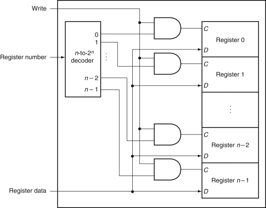
# Subtraction, Sequential Logic --- CS 130 // 2024-10-08 <!--=====================================================================--> ## Schedule Heads up * Assignment 5 due tonight * Fall break next Tuesday * Assignment 6 due next Thursday * Exam 2: October 22nd <!--=====================================================================--> # Review: Adder and ALU Start <!-- .slide: data-background="#004477" --> <!--=====================================================================--> ## 4-Bit Adder and a Start to an ALU <div class="twocolumn" style="font-size: 60%"> <div>  <!-- .element width="550px" --> </div> <div>  <!-- .element width="550px" --> </div> <!--=====================================================================--> <!-- .slide: data-background="#004477" --> # Subtraction <!--=====================================================================--> ## Subtraction - You can use the same adder circuitry to support subtraction - convert **B** into it's negative value - flip all the bits (NOT gate) - add 1 (give a 1 to **Cin**) [Adder/Subtractor test vector](../../assets/addersubtractor4bit_test_vector.txt) <!--=====================================================================--> ## Supporting `slt` You can even use your adder for *set on less than* - set the adder to do subtraction - look at the highest bit of the result + if it is 1, then the subtraction result was negative, so set result to 1 + if it is 0, then the subtraction result was not negative, so set result to 0 <!--=====================================================================--> ## Exercise - Work on getting subtraction and `slt` working in your 4-bit ALU <!--=====================================================================--> ## Assignment - [Assignment 6](../../assignments/assignment-6) - make a 32-bit ALU - `add`, `sub`, `and`, `or`, `not`, `xor`, `slt`, and anything else you want - you can use Logisim's built-in components - try not to duplicate circuitry for `add`, `sub`, and `slt`. - submit screenshots of circuits *and* test vector (with comments) <!--=====================================================================--> # Sequential Logic <!-- .slide: data-background="#004477" --> <!--=====================================================================--> ## Combinational VS Sequential - A **combinational circuit** is: + Relies solely on the input to resolve its output + Stateless / memoryless / doesn't depend on previous states --- - A **sequential circuit** is: + Relies on input *and* current state to resolve its output + Has memory <!--=====================================================================--> ## S-R Latch <div class="twocolumn"> <div> - A "set reset" latch is implemented with <img src='/Fall2024/CS130/assets/images/COD/sr-latch.png' alt="S-R latch diagram" /> - Let's fill in the truth table together </div> <div style="font-size: 70%"> <table> <tbody> <tr><th>$S$</th><th>$R$</th><th>$Q$</th><th>$\overline{Q}$</th><th>$Q_\text{next}$</th><th>$\overline{Q}_\text{next}$</th></tr> <tr> <td>0</td> <td>0</td> <td>0</td><td>1</td><td></td><td></td></tr> <tr> <td>0</td> <td>0</td> <td>1</td><td>0</td><td></td><td></td></tr> <tr> <td>1</td> <td>0</td> <td>0</td><td>1</td><td></td><td></td></tr> <tr> <td>1</td> <td>0</td> <td>1</td><td>0</td><td></td><td></td></tr> <tr> <td>0</td> <td>1</td> <td>0</td><td>1</td><td></td><td></td></tr> <tr> <td>0</td> <td>1</td> <td>1</td><td>0</td><td></td><td></td></tr> </tbody> </table> </div> </div> <!--=====================================================================--> ## D Latch <div class="twocolumn"> <div> - A "data" latch is implemented with <img src='/Fall2024/CS130/assets/images/COD/d-latch.png' alt="D latch diagram" /> - Let's fill in the truth table together </div> <div style="font-size: 90%"> <table> <tbody> <tr><th>$C$</th><th>$D$</th><th>$Q_\text{next}$</th></tr> <tr> <td>0</td> <td>0</td> <td></tr> <tr> <td>0</td> <td>1</td> <td></tr> <tr> <td>1</td> <td>0</td> <td></tr> <tr> <td>1</td> <td>1</td> <td></tr> </tbody> </table> </div> </div> <!--=====================================================================--> ## Clocks - Latches are controlled by clocks that regularly trigger <div class="twocolumn"> <div>  </div> <div>  </div> </div> <!--=====================================================================--> ## Exercise - Experiment with these in Logisim - How can you get it to store a 1 in the latch? - How can you get it to store a 0 in the latch? <div class="twocolumn"> <div>  </div> <div>  </div> </div> <!--=====================================================================--> ## D Flip Flop <div style="font-size: 90%"> - A (falling edge-triggered) **D flip flop** can be implemented with two D latches in series - This configuration creates a **delay** so that the output is only changed on the **falling edge** of the clock <img src='/Fall2024/CS130/assets/images/COD/d-flip-flop.png' alt="D flip flop diagram" /> - a rising edge-triggered flip flop can be constructed similarly </div> <!--=====================================================================--> ## Registers - A **register** is a multi-bit memory component - Registers are commonly implemented with an array of D flip flops <!--=====================================================================--> ## Register Files - A **register file** consists of an array of registers that can be read and written to 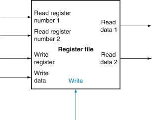 <!----------------------------------> ## Register Files - **Reading** is implemented with multiplexers 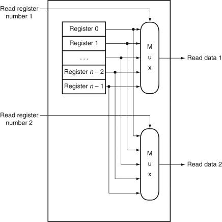 <!----------------------------------> ## Register Files - **Writing** is implemented with a decoder